
Japanese startup Gaianixx announced on March 2 that it has secured 2 billion yen (approximately $13 million USD) in the 1st round of its Series C funding, which develops Multi-functional Interlayers for semiconductors.
The company was founded in 2021 as a startup originating from the Tabata Laboratory at the Graduate School of Engineering, The University of Tokyo.
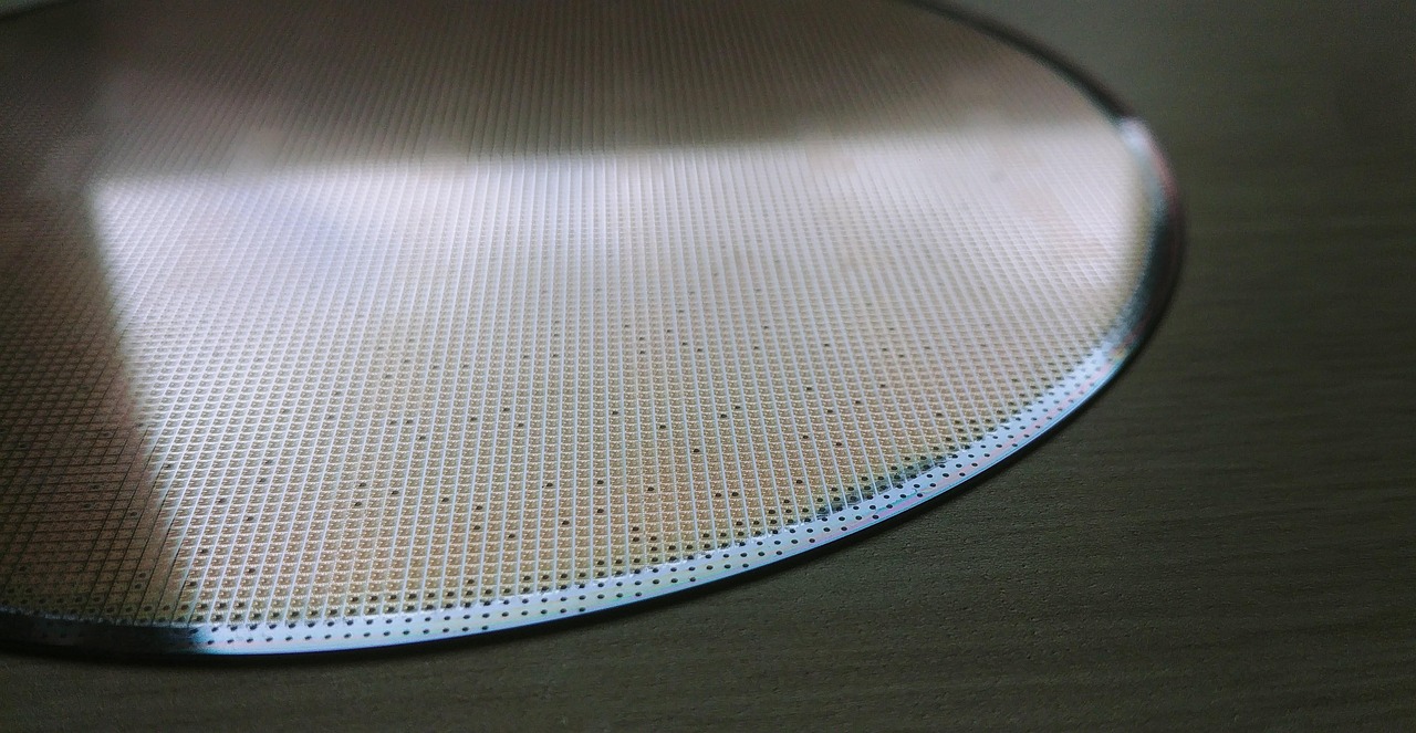
How Does Gaianixx Improve Yield in Semiconductor Manufacturing?
“Yield” is one of the most commonly used terms in semiconductor manufacturing. It refers to the proportion of finished products that are free of defects — a high yield means fewer defective units.
There are many causes of poor yield, and one of them is a mismatch between the crystal lattice spacing of the semiconductor substrate and the thin film deposited on top of it. This is known as lattice mismatch. When lattice mismatch occurs, the film can crack or warp, resulting in defective products.
To address this challenge, Gaianixx has developed the “Multi-functional Interlayer.” It first matches the atomic spacing of the interlayer to that of the substrate crystal, and then further aligns the atomic spacing with additional material layers on top, thereby improving yield.
This is made possible by the application of Martensite to semiconductors. Martensite is a hard crystal structure formed when iron or steel is quenched. While the specific manufacturing process has not been disclosed, Gaianixx is believed to apply a process equivalent to the quenching of steel within the semiconductor domain.
JX Advanced Metals, Mitsui Kinzoku, and Others Participate
Ten investors participated in the Series C 1st Round. Among corporate strategic investors, JX Advanced Metals, ALCONIX, Mitsui Kinzoku-SBI Material Innovation Fund Ⅱ, and Toray International took part.
The funds will be used for the full-scale launch of the Yamanashi Technical Center, the company’s development hub, operation of its pilot line, talent acquisition, and intellectual property strategy.
Gaianixx CEO Kento Nakao commented: “We will continue to provide innovative manufacturing solutions to device makers around the world, with the aim of contributing to a semiconductor ecosystem that accelerates growth.”