
The company is a Nagoya University-based startup founded in 2015.
A Photocathode That Achieves Both Precision and Speed in Semiconductor Inspection
“Moore’s Law” describes the pace of semiconductor advancement, predicting that integration density doubles roughly every one and a half to two years. While some argue that Moore’s Law is approaching its limits, semiconductors continue to advance not only through miniaturization but also through increased layering—and for now, integration density continues to rise.
As a result, semiconductor inspection—the process of checking chips for defects—becomes exceedingly difficult. PeS describes the challenge of inspecting today’s increasingly miniaturized and multi-layered semiconductors as “comparable to finding a single ant hidden somewhere in a vast metropolis packed with skyscrapers.”
Semiconductor inspection relies on scanning with an electron beam, but conventionally, narrowing the beam to improve inspection precision reduces current strength, slowing the scan. Conversely, increasing speed comes at the cost of precision.
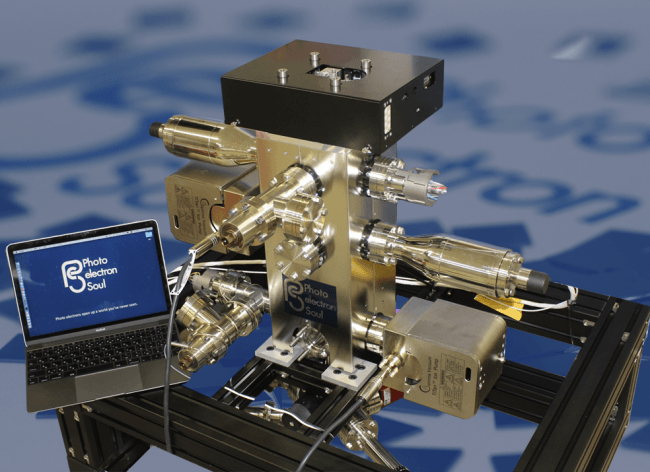
To address this, PeS developed a semiconductor-based photocathode. The photocathode is the source from which the beam is generated; conventional designs used metal. By applying high current even to a narrow beam, the semiconductor photocathode achieves both scanning precision and speed.
While the name of the client has not been disclosed for confidentiality reasons, PeS has announced that it received an order for an electron beam generation system from a semiconductor inspection equipment manufacturer in 2019.
Targeting Customers in Kumamoto and Taiwan
The March 2026 funding round included participation from Shibaura Mechatronics, Higin Capital, and Hotung Venture Capital.
The company has cited the following three areas for use of proceeds.
- Strengthening mass production and maintenance capabilities for the semiconductor photocathode electron beam generation system
- Accelerating development investment in next-generation electron beam applications (inspection, metrology, advanced patterning, etc.)
- Strengthening sales and support capabilities to expand the global customer base
Higin Capital is the venture capital arm of Higo Bank, a regional bank in Kumamoto Prefecture where TSMC has established a factory. Hotung Venture GroupMeanwhile, Hotung Venture Group is a VC based in Taiwan, home to TSMC’s headquarters. Against this backdrop of strategically aligned investors, the company intends to advance its customer development efforts.
No comments from the company’s management have been made public.